- 您现在的位置:买卖IC网 > Sheet目录491 > NTMS4840NR2G (ON Semiconductor)MOSFET N-CH 30V 4.5A 8SOIC
�� �
�
�NTMS4840N�
�Power� MOSFET�
�30� V,� 7.5� A,� Single� N� ?� Channel,� SOIC� ?� 8�
�Features�
�?� Low� R� DS(on)� to� Minimize� Conduction� Losses�
�?� Low� Capacitance� to� Minimize� Driver� Losses�
�?� Optimized� Gate� Charge� to� Minimize� Switching� Losses�
�?� SOIC� ?� 8� Surface� Mount� Package� Saves� Board� Space�
�?� These� Devices� are� Pb� ?� Free,� Halogen� Free/BFR� Free� and� are� RoHS�
�Compliant�
�Applications�
�?� DC� ?� DC� Converters�
�?� Printers�
�MAXIMUM� RATINGS� (T� J� =� 25� °� C� unless� otherwise� stated)�
�V� (BR)DSS�
�30� V�
�http://onsemi.com�
�R� DS(on)� Max�
�24� m� W� @� 10� V�
�36� m� W� @� 4.5� V�
�N� ?� Channel�
�D�
�I� D� Max�
�7.5� A�
�Rating�
�Drain� ?� to� ?� Source� Voltage�
�Gate� ?� to� ?� Source� Voltage�
�Symbol�
�V� DSS�
�V� GS�
�Value�
�30�
�±� 20�
�Unit�
�V�
�V�
�Continuous� Drain�
�Current� R� q� JA� (Note� 1)�
�Power� Dissipation�
�R� q� JA� (Note� 1)�
�T� A� =� 25� °� C�
�T� A� =� 70� °� C�
�T� A� =� 25� °� C�
�I� D�
�P� D�
�5.5�
�4.4�
�1.14�
�A�
�W�
�G�
�S�
�T� A� =� 70� °� C�
�Continuous� Drain�
�Current� R� q� JA� (Note� 2)�
�Power� Dissipation�
�R� q� JA� (Note� 2)�
�Continuous� Drain�
�Current� R� q� JA� t� <� 10� s�
�(Note� 1)�
�Power� Dissipation�
�R� q� JA� t� <� 10� s� (Note� 1)�
�Pulsed� Drain� Current�
�T� A� =� 25� °� C�
�Steady�
�State� T� A� =� 25� °� C�
�T� A� =� 25� °� C�
�T� A� =� 70� °� C�
�T� A� =� 25� °� C�
�T� A� =� 25� °� C,�
�t� p� =� 10� m� s�
�I� D�
�P� D�
�I� D�
�P� D�
�I� DM�
�4.5�
�3.5�
�0.68�
�7.5�
�6.0�
�1.95�
�38�
�A�
�W�
�A�
�W�
�A�
�1�
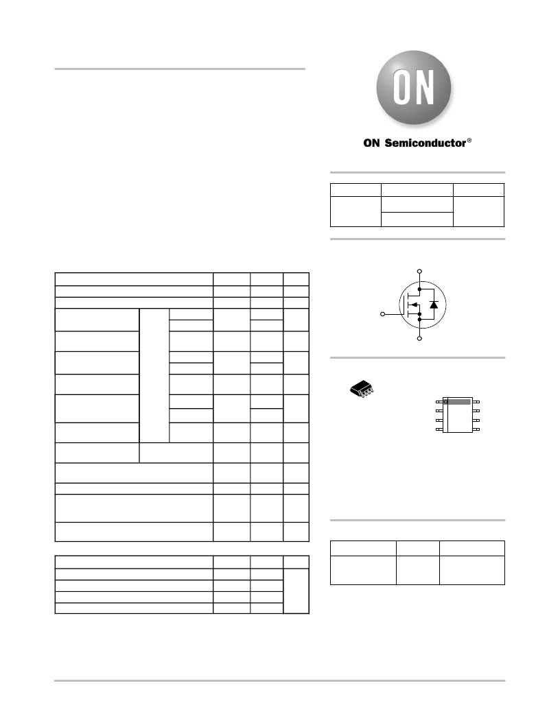
�SO� ?� 8�
�CASE� 751�
�STYLE� 12�
�MARKING� DIAGRAM�
�&� PIN� ASSIGNMENT�
�1� 8�
�Source� Drain�
�Source� Drain�
�Source� Drain�
�Gate� Drain�
�Top� View�
�Operating� Junction� and� Storage� Temperature�
�Source� Current� (Body� Diode)�
�Single� Pulse� Drain� ?� to� ?� Source� Avalanche�
�Energy� T� J� =� 25� °� C,� V� DD� =� 30� V,� V� GS� =� 10� V,�
�I� L� =� 7.5� A� pk� ,� L� =� 1.0� mH,� R� G� =� 25� W�
�T� J� ,� T� STG�
�I� S�
�EAS�
�?� 55� to�
�+150�
�2.0�
�28�
�°� C�
�A�
�mJ�
�S4840�
�A�
�Y�
�WW�
�G�
�=� Device� Code�
�=� Assembly� Location�
�=� Year�
�=� Work� Week�
�=� Pb� ?� Free� Package�
�Lead� Temperature� for� Soldering� Purposes�
�(1/8� ″� from� case� for� 10� s)�
�THERMAL� RESISTANCE� RATINGS�
�T� L�
�260�
�°� C�
�ORDERING� INFORMATION�
�Shipping� ?�
�Device�
�Package�
�Rating�
�Junction� ?� to� ?� Ambient� –� Steady� State� (Note� 1)�
�Symbol�
�R� q� JA�
�Max�
�110�
�Unit�
�NTMS4840NR2G�
�SOIC� ?� 8�
�(Pb� ?� Free)�
�2500/Tape� &� Reel�
�°� C/W�
�Junction� ?� to� ?� Ambient� –� t� ≤� 10� s� (Note� 1)� R� q� JA� 64�
�Junction� ?� to� ?� FOOT� (Drain)� R� q� JF� 40�
�Junction� ?� to� ?� Ambient� –� Steady� State� (Note� 2)� R� q� JA� 183.5�
�Stresses� exceeding� Maximum� Ratings� may� damage� the� device.� Maximum�
�Ratings� are� stress� ratings� only.� Functional� operation� above� the� Recommended�
�Operating� Conditions� is� not� implied.� Extended� exposure� to� stresses� above� the�
�Recommended� Operating� Conditions� may� affect� device� reliability.�
�1.� Surface� ?� mounted� on� FR4� board� using� 1� inch� sq� pad� size,� 1� oz� Cu.�
�2.� Surface� ?� mounted� on� FR4� board� using� the� minimum� recommended� pad� size.�
�?For� information� on� tape� and� reel� specifications,�
�including� part� orientation� and� tape� sizes,� please�
�refer� to� our� Tape� and� Reel� Packaging� Specification�
�Brochure,� BRD8011/D.�
�?� Semiconductor� Components� Industries,� LLC,� 2009�
�September,� 2009� ?� Rev.� 1�
�1�
�Publication� Order� Number:�
�NTMS4840N/D�
�发布紧急采购,3分钟左右您将得到回复。
相关PDF资料
NTMS4872NR2G
MOSFET N-CH 30V 6A 8-SOIC
NTMS4873NFR2G
MOSFET N-CH SGL 30V 8-SOIC
NTMS4916NR2G
MOSFET N-CH 30V 11.4A SO8 FL
NTMS4917NR2G
MOSFET N-CH 30V 10.2A SO8 FL
NTMS4920NR2G
MOSFET N-CH 30V 10.6A 8SOIC
NTMS4935NR2G
MOSFET N-CH 30V 10A 8SOIC
NTMS4937NR2G
MOSFET N-CH 30V 8.6A 8SOIC
NTMS4N01R2G
MOSFET N-CH 20V 3.3A 8-SOIC
相关代理商/技术参数
NTMS4872N
制造商:ONSEMI 制造商全称:ON Semiconductor 功能描述:Power MOSFET 30 V, 10.2 A, N−Channel, SO−8
NTMS4872NR2G
功能描述:MOSFET NFET SO8 30V 10.2A 13.5mOhm RoHS:否 制造商:STMicroelectronics 晶体管极性:N-Channel 汲极/源极击穿电压:650 V 闸/源击穿电压:25 V 漏极连续电流:130 A 电阻汲极/源极 RDS(导通):0.014 Ohms 配置:Single 最大工作温度: 安装风格:Through Hole 封装 / 箱体:Max247 封装:Tube
NTMS4873NF
制造商:ONSEMI 制造商全称:ON Semiconductor 功能描述:Power MOSFET 30 V, 11.5 A, N−Channel, SO−8
NTMS4873NFR2G
功能描述:MOSFET NFET SO8 30V 11.7A 12MOHM RoHS:否 制造商:STMicroelectronics 晶体管极性:N-Channel 汲极/源极击穿电压:650 V 闸/源击穿电压:25 V 漏极连续电流:130 A 电阻汲极/源极 RDS(导通):0.014 Ohms 配置:Single 最大工作温度: 安装风格:Through Hole 封装 / 箱体:Max247 封装:Tube
NTMS4916N
制造商:ONSEMI 制造商全称:ON Semiconductor 功能描述:Power MOSFET 30 V, 11.6 A, N?Channel, SO?8 Low RDS(on) to Minimize Conduction Losses
NTMS4916NR2G
功能描述:MOSFET NFET SO8 30V 11.4A 9MOHM RoHS:否 制造商:STMicroelectronics 晶体管极性:N-Channel 汲极/源极击穿电压:650 V 闸/源击穿电压:25 V 漏极连续电流:130 A 电阻汲极/源极 RDS(导通):0.014 Ohms 配置:Single 最大工作温度: 安装风格:Through Hole 封装 / 箱体:Max247 封装:Tube
NTMS4917N
制造商:ONSEMI 制造商全称:ON Semiconductor 功能描述:Power MOSFET 30 V, 10.5 A, N?Channel, SO?8 Low RDS(on) to Minimize Conduction Losses
NTMS4917NR2G
功能描述:MOSFET NFET SO8 30V 10.2A 11MOHM RoHS:否 制造商:STMicroelectronics 晶体管极性:N-Channel 汲极/源极击穿电压:650 V 闸/源击穿电压:25 V 漏极连续电流:130 A 电阻汲极/源极 RDS(导通):0.014 Ohms 配置:Single 最大工作温度: 安装风格:Through Hole 封装 / 箱体:Max247 封装:Tube